LinkBack URL
 About LinkBacks
Read more.Indicates an updated Intel reference document for software developers.


Read more.Indicates an updated Intel reference document for software developers.
Only a limited amount of things Intel can yo in an attempt to combat Ryzen (thingscthey can market) in the short term.
They'redesperate
Even if true, let's not put a negative spin on it. Things like this are a welcome reminder of why competition is so important. Long may it continueOriginally Posted by Yoyoyo69

Corky34 (21-10-2017)
what is AMD's alternative to AVX512?

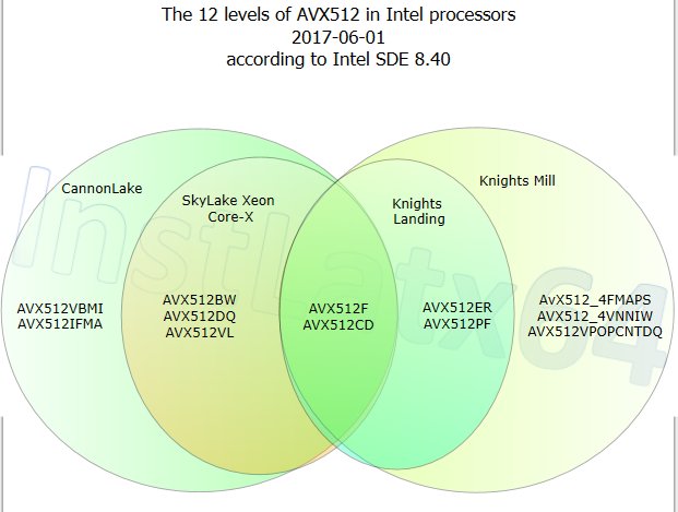
If people read the article carefully,you will notice multiple different versions of AVX512 - this is because the versions used by CPUs and Intel's own accelerator cards do not necessarily overlap,and it has been segmented massively dependent on SKU. Its also been known for a while Cannonlake would get AVX512.
So I wonder if this will mean Intel,will try and standardise AVX512 versions moving forwward??
Also the reason they have probably waited until 10NM to rollout AVX512 on consumer CPUs can be kind of understand from this line from an AT review of SKLX:
AVX-512 register file could probably fit a whole Atom coreAMD current alternative to AVX256 is a version of FMA,AFAIK,but Ryzen does AVX256 at a lower throughput than Intel CPUs,as apparently it does take up a reasonable amount of die area to implement,and AMD uses a smaller physical core than SKL/KL/CFL. AFAIK,they don't support AVX512 but it is very niche currently - even AVX256 support is not very common in a lot of consumer/commercial applications but a some do and Intel is noticeably faster.
For games I am uncertain how much it will make a difference though - AFAIK,the consoles can only run AVX like applications in 128 bit,so don't support 256 bit and 512 bit very well.
Edit!!
A better explanation of all of this by Agner:
http://www.agner.org/optimize/blog/read.php?i=838
The new Ryzen processor from AMD represents a complete redesign of the CPU microarchitecture. This is the first of a series of "Zen" architecture processors. I must say that this redesign is a quite successful one which puts AMD back in the game after several years of lagging behind Intel in performance.
The Ryzen has a micro-operation cache which can hold 2048 micro-operations or instructions. This is sufficient to hold the critical innermost loop in most programs. There has been discussions of whether the Ryzen would be able to run four instructions per clock cycle or six, because the documents published by AMD were unclear at this point. Well, my testing shows that it was not four, and not six, but five. As long as the code is running from the micro-operations cache, it can execute five instructions per clock, where Intel has only four. Code that doesn't fit into the micro-operations cache run from the traditional code cache at a maximum rate of four instructions per clock. However, the rate of fetching code from the code cache is not 32 bytes per clock, as some documents seem to indicate, but mostly around 16 bytes per clock. The maximum I have seen is 17.3 bytes per clock. This is a likely bottleneck since most instructions in vector code are more than four bytes long.
The combination of a compare instruction and a conditional jump can be fused together into a single micro-op. This makes it possible to execute a tiny loop with up to six instructions in one clock cycle per iteration. Except for tiny loops, the throughput for jumps is one jump per two clock cycles if the jump is taken, or two not-taken jumps per clock cycle.
256-bit vector instructions (AVX instructions) are split into two micro-ops handling 128 bits each. Such instructions take only one entry in the micro-operation cache. A few other instructions also generate two micro-ops. The maximum throughput of the micro-op queue after the decoders is six micro-ops per clock. The stream of micro-ops from this queue are distributed between ten pipelines: four pipes for integer operations on general purpose registers, four pipes for floating point and vector operations, and two for address calculation. This means that a throughput of six micro-ops per clock cycle can be obtained if there is a mixture of integer and vector instructions.
Let us compare the execution units of AMD's Ryzen with current Intel processors. AMD has four 128-bit units for floating point and vector operations. Two of these can do addition and two can do multiplication. Intel has two 256-bit units, both of which can do addition as well as multiplication. This means that floating point code with scalars or vectors of up to 128 bits will execute on the AMD processor at a maximum rate of four instructions per clock (two additions and two multiplications), while the Intel processor can do only two. With 256-bit vectors, AMD and Intel can both do two instructions per clock. Intel beats AMD on 256-bit fused multiply-and-add instructions, where AMD can do one while Intel can do two per clock. Intel is also better than AMD on 256-bit memory writes, where Intel has one 256-bit write port while the AMD processor has one 128-bit write port. We will soon see Intel processors with 512-bit vector support, while it might take a few more years before AMD supports 512-bit vectors. However, most of the software on the market lags several years behind the hardware. As long as the software uses only 128-bit vectors, we will see the performance of the Ryzen processor as quite competitive. The AMD can execute six micro-ops per clock while Intel can do only four. But there is a problem with doing so many operations per clock cycle. It is not possible to do two instructions simultaneously if the second instruction depends on the result of the first instruction, of course. The high throughput of the processor puts an increased burden on the programmer and the compiler to avoid long dependency chains. The maximum throughput can only be obtained if there are many independent instructions that can be executed simultaneously.
This is where simultaneous multithreading comes in. You can run two threads in the same CPU core (this is what Intel calls hyperthreading). Each thread will then get half of the resources. If the CPU core has a higher capacity than a single thread can utilize then it makes sense to run two threads in the same core. The gain in total performance that you get from running two threads per core is much higher in the Ryzen than in Intel processors because of the higher throughput of the AMD core (except for 256-bit vector code).
The Ryzen is saving power quite aggressively. Unused units are clock gated, and the clock frequency is varying quite dramatically with the workload and the temperature. In my tests, I often saw a clock frequency as low as 8% of the nominal frequency in cases where disk access was the limiting factor, while the clock frequency could be as high as 114% of the nominal frequency after a very long sequence of CPU-intensive code. Such a high frequency cannot be obtained if all eight cores are active because of the increase in temperature.
The varying clock frequency was a big problem for my performance tests because it was impossible to get precise and reproducible measurements of computation times. It helps to warm up the processor with a long sequence of dummy calculations, but the clock counts were still somewhat inaccurate. The Time Stamp Counter (TSC), which is used for measuring the execution time of small pieces of code, is counting at the nominal frequency. The Ryzen processor has another counter called Actual Performance Frequency Clock Counter (APERF) which is similar to the Core Clock Counter in Intel processors. Unfortunately, the APERF counter can only be read in kernel mode, unlike the TSC which is accessible to the test program running in user mode. I had to calculate the actual clock counts in the following way: The TSC and APERF counters are both read in a device driver immediately before and after a run of the test sequence. The ratio between the TSC count and the APERF count obtained in this way is then used as a correction factor which is applied to all TSC counts obtained during the running of the test sequence. This method is awkward, but the results appear to be quite precise, except in the cases where the frequency is varying considerably during the test sequence. My test program is available at www.agner.org/optimize/#testp
AMD has a different way of dealing with instruction set extensions than Intel. AMD keeps adding new instructions and remove them again if they fail to gain popularity, while Intel keeps supporting even the most obscure and useless undocumented instructions dating back to the first 8086. AMD introduced the FMA4 and XOP instruction set extensions with Bulldozer, and some not very useful extensions called TBM with Piledriver. Now they are dropping all these again. XOP and TBM are no longer supported in Ryzen. FMA4 is not officially supported on Ryzen, but I found that the FMA4 instructions actually work correctly on Ryzen, even though the CPUID instruction says that FMA4 is not supported.
Detailed results and list of instruction timings are in my manuals: www.agner.org/optimize/#manuals.
Last edited by CAT-THE-FIFTH; 21-10-2017 at 11:13 AM.
Cannon lake and Z390. i'm in.
Another hit to Ryzen....Ryzen looks old now

Not really, the AVX512 instructions only made sense for Larrabee where a cut down Atom style core which can only do in-order dual issue of instructions means you need to pack as much punch into each instruction as possible. That is real CISC thinking but works in that corner case where you know that the cpu will only ever run vector code.
What would make sense here is if Intel take 512 bit AVX instructions and do them in two 256 bit chunks to make it software compatible with their MIC range of accelerators so you can compile and test on a desktop CPU and then go run your code on a supercomputer with confidence that your slot won't be wasted. That would add little to the cost of the chip.
If this is adding 512 bit vector units to the desktop range, I have to be surprised. These things are significant, and Intel cores are already floating point monsters in terms of their basic spec and how much silicon goes into their FP ability. Intel do have Xeon cpus which already do these sort of instructions, but ISTR they clock lower than the vanilla cores without AVX512 support (no surprise, https://en.wikipedia.org/wiki/Amdahl%27s_law) so I have to wonder if the silicon would be better spent on either more L3 cache or twice the number of 256 bit AVX units as that could benefit existing software.
There are currently 1 users browsing this thread. (0 members and 1 guests)
 Posting Permissions

 Reply With Quote