Page 99 of 137 FirstFirst ... 495969798996979899100101102109119129 ... LastLast
Results 1,569 to 1,584 of 2179

Thread: AMD - Zen chitchat

  1. #1569
    Senior Member
    Join Date
    Dec 2013
    Posts
    3,526
    Thanks
    504
    Thanked
    468 times in 326 posts

    Re: AMD - Zen chitchat

    Quote Originally Posted by watercooled View Post
    That's what I was getting at originally, there is no one thing you can point at and say 'thats the IF'. And back to the original debate, the chiplets will have a SerDes, similar to IFOP blocks, to communicate with the NorthBridge. They need that because they obviously have to extend the fabric off the die to be able to communicate with the NorthBridge, you can't just strip the fabric out because then there would be no way to communicate between CCX blocks on-die (if there are multiple) and between different dies on-package. On-package blocks don't have to be as big despite doing much the same thing, due to smaller distances involved, as you can see in the highlighted die shot you posted.

    The off-package blocks will be on the NorthBridge die, and that's the whole reasoning behind doing this - those large off-socket SerDes blocks take up a heck of a lot of die space and don't scale well with smaller nodes so it makes absolute sense to do what AMD are doing. This is precisely the sort of modularity that AMD have been working towards with IF and I very much doubt they'll be the last to do this. Even Intel are going multi-die on Xeon now!
    Yes, re: IF and these chiplets having IFOP SerDes'.

    Although how much more or less they have is unknown currently, some people said AMD mentioned each chiplet retains PCIe connectivity and it may only be the memory control that's been moved to the I/O die, at least that's what I've read as I've not watched AMD's event myself. If so that would mean only the Southbridge and USB block locations are unknown, the SATA/Ethernet controller seems to share one of the PCIe blocks, the two remaining unknown block locations don't actually take up much die area. Has TSCM achieved really good density with 7nm as the chiplet dies seem a lot smaller than their 14/12nm Zeppelin dies despite possibly only removing the memory controllers.

    It would also mean that I/O die is way oversized to contain said memory controllers (is it 8?) and maybe a USB and Southbridge block so that lends validity to a suspected lump of L4 cache, 64 cores would already have 128Mb of L3 so maybe they've added 3-400Mb of L4.

    Quote Originally Posted by DanceswithUnix View Post
    I don't believe they are two different competing things, just a representation that a fabric has more than one job to do. We live in a complicated and messy world, and often the best engineering solutions are the ones that reflect that rather than the ones that are nice and simple.

    Really I think you are over thinking this. AMD have a fabric that connects blocks together within a die, which they can also drive between the die of an MCM and between sockets in a multi socket system. It goes through conversion blocks along the way. Unless you work in AMD in the right department, you aren't going to pull it apart more than that.
    I wouldn't call them competing i was just trying to clarify what we mean when talking about IF, if i remember correctly the data and control fabric are two separate layers with one being laid down on the BEOL and the other on the FEOL, I'll try to find where i may have read that and edit this post to add a link after I've re-read some stuff.

    EDIT: After having re-read a load of stuff on-and-off today i suspect i confused what i read about Intel's fab with AMD's...(this wikiichip article talks about "The top of the die is called the North Cap and it contains all of the I/O PHYs, I/O agents, serial IP ports, and the fuse unit." So I'm guessing i mixed the two up.

    It's not over-thinking this, I'm trying to piece together the limited information we have about current design and the recently announced change in an attempt to fill in the blanks...Sorry if I've annoyed you it's just i find it interesting to speculate what they've changed and if these changes will filter down to us plebs, does this change in design make sense when it comes to lower core count processors and all those other unanswered question that come from such a change.

    Quote Originally Posted by DanceswithUnix View Post
    I have yet to see anything meaningful written about the control fabric. It's all hand waving, broken links and irrelevances. However, any connection system requires things like boot configuration and out of band signals like interrupts. Getting that off the critical path of data handling makes a lot of sense, so I presume that is what they are doing. I suspect in this case the control plane just isn't considered interesting enough to document. Much like in a Ferrari people don't write much about the electric motors that wind the windows, they just concentrate on the big one that drives the wheels.
    Yea there's not much written about that is there. It's not much but this wiki fuse article has some info, at least more than the no information that most articles contain. If i get the time I'll try to find something more substantive and update this post with a link but it's Saturday night and i don't fancy spending it reading so maybe that's something for Sunday morning.

    Quote Originally Posted by Foxdragon View Post
    Does ryzen function more of a system on chip or more general cpu?
    Most people, including AMD, describe it as a SoC.
    Last edited by Corky34; 11-11-2018 at 05:13 PM.

  2. #1570
    Senior Member watercooled's Avatar
    Join Date
    Jan 2009
    Posts
    11,478
    Thanks
    1,541
    Thanked
    1,029 times in 872 posts

    Re: AMD - Zen chitchat

    I'd be surprised if the chiplets retain full* PCIe connectivity - any source for that? I watched most of that part of the presentation (apart from when it cut out) and didn't hear anything like that.

    *I say full, because IIRC on Zen1, IFIS and PCIe share the block and it can be configured in either mode. I.e. on desktop or a single-socket EPYC system they're set as PCIe, but in a multi-socket system, one of the two links from each die is used as an IF link to the other socket. One reason why that block might be a full-blown PCIe block is if it's the same sort of hybrid - on EPYC2 it's purely an IF link, but on desktop it could be configured as PCIe. But I don't see that as particularly likely - that sort of block would be far larger than the sort needed for on-package links and would have some tough trade-offs between number of links and space savings on the dies. It seems hardly worth it if pretty much all they've moved off-die is the IMC, and that central die is far too big for that. I'm eagerly awaiting more details but plenty are speculating what's on there e.g. the possibility of an L4 cache.

    That also leads into your next comment about how small the chiplet die is - 7nm is a proper shrink from 16/14/12nm so there's that, but the Zen2 cores will still be 'larger' in terms of transistors, so I agree the chiplets seem too small if AMD had only stripped the IMC - it doesn't add up, just like the IO chip being overly large if that were the case...

    I've also read a few people speculating about the decisions around using GloFo 14nm for the IO chip to satisfy WSA - unless AMD knew well in advance of everyone else about GloFo's plans to abandon 7nm, I doubt there's been nearly enough time to change the designs like that - people still don't realise just how long silicon design takes, it's certainly not something you can change overnight.

  3. #1571
    Senior Member watercooled's Avatar
    Join Date
    Jan 2009
    Posts
    11,478
    Thanks
    1,541
    Thanked
    1,029 times in 872 posts

    Re: AMD - Zen chitchat

    I've just checked and SA have an article up and addresses some of these questions: https://semiaccurate.com/2018/11/09/...eed-a-monster/

    It's worth a full read, but amongst other things he claims 8 core CCXs (so one per die), and hence each die has a point-to-point IF link to the IO chip. He also says all IO goes through this, including PCIe. It's not official from AMD, but Charlie tends to not make random claims...

  4. #1572
    Senior Member
    Join Date
    Dec 2013
    Posts
    3,526
    Thanks
    504
    Thanked
    468 times in 326 posts

    Re: AMD - Zen chitchat

    Quote Originally Posted by watercooled View Post
    I'd be surprised if the chiplets retain full* PCIe connectivity - any source for that? I watched most of that part of the presentation (apart from when it cut out) and didn't hear anything like that.
    I read it on Anandtech and Nextplatform but having re-read them i think they and i maybe conflating the move to PCIe 4.0, AMD not mentioning if PCIe is part of the I/O die, and assumed that the chiplets have retained them. However after reading your post and remembering IFOP and IFIS are electrically different buses it's clear Nextplatform got it wrong as they say IF uses PCIe and that's only partially true, and Andantech seem to have made a leap of faith.

    What you say makes much more sense IMO.

  5. #1573
    Senior Member
    Join Date
    Dec 2013
    Posts
    3,526
    Thanks
    504
    Thanked
    468 times in 326 posts

    Re: AMD - Zen chitchat

    Interesting interview with Papermaster on Anandtech, needless to say he doesn't give much away.

  6. #1574
    Senior Member
    Join Date
    Mar 2005
    Posts
    4,946
    Thanks
    171
    Thanked
    388 times in 315 posts
    • badass's system
      • Motherboard:
      • ASUS P8Z77-m pro
      • CPU:
      • Core i5 3570K
      • Memory:
      • 32GB
      • Storage:
      • 1TB Samsung 850 EVO, 2TB WD Green
      • Graphics card(s):
      • Radeon RX 580
      • PSU:
      • Corsair HX520W
      • Case:
      • Silverstone SG02-F
      • Operating System:
      • Windows 10 X64
      • Monitor(s):
      • Del U2311, LG226WTQ
      • Internet:
      • 80/20 FTTC

    Re: AMD - Zen chitchat

    Anyone else think Intel are getting desperate now?

    https://www.anandtech.com/show/13586...rmance-numbers

    Future processor extrapolated benchmarks being compared to a 2017 processor.

    It really looks like AMD will take the server performance crown next year.
    "In a perfect world... spammers would get caught, go to jail, and share a cell with many men who have enlarged their penises, taken Viagra and are looking for a new relationship."

  7. #1575
    Senior Member
    Join Date
    Dec 2013
    Posts
    3,526
    Thanks
    504
    Thanked
    468 times in 326 posts

    Re: AMD - Zen chitchat

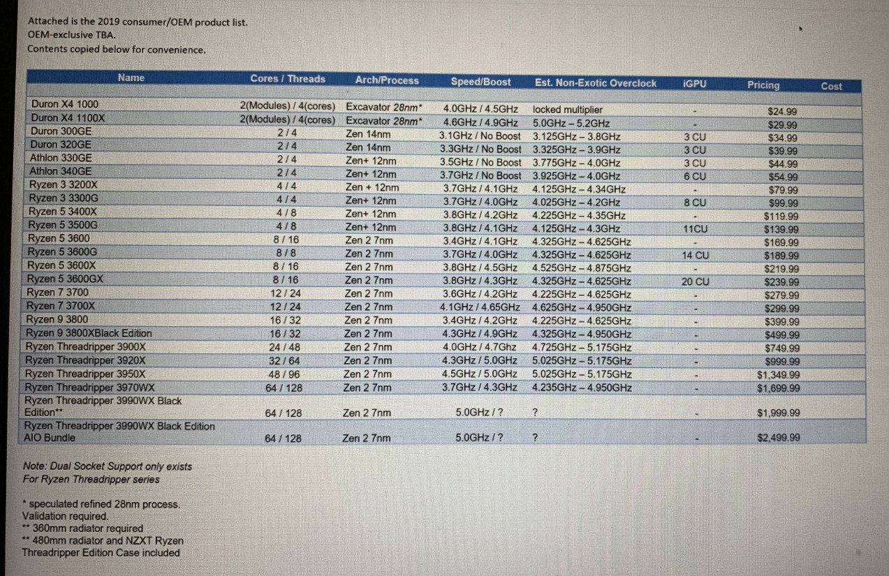
    Take a super big pinch of salt with this but apparently it shows the Ryzen 3 lineup, via Techpowerup.


  8. #1576
    Senior Member watercooled's Avatar
    Join Date
    Jan 2009
    Posts
    11,478
    Thanks
    1,541
    Thanked
    1,029 times in 872 posts

    Re: AMD - Zen chitchat

    Aye, bucket of salt applied, but IMO it's fairly reasonable if AMD chose to do. The only things I'd be wondering about is clock speeds and power at those clocks, but maybe 7nm and chiplet binning has helped a fair bit with that.

  9. #1577
    Senior Member watercooled's Avatar
    Join Date
    Jan 2009
    Posts
    11,478
    Thanks
    1,541
    Thanked
    1,029 times in 872 posts

    Re: AMD - Zen chitchat

    An interesting tidbit: https://www.techpowerup.com/250286/t...demand-weakens

    Less capacity competition for AMD then!

  10. #1578
    Senior Member
    Join Date
    Oct 2018
    Posts
    415
    Thanks
    58
    Thanked
    32 times in 30 posts
    • PC-LAD's system
      • Motherboard:
      • X370 GT7
      • CPU:
      • R5 3600 @ 4.3GHz
      • Memory:
      • 4*4 GB TG Delta @2933
      • Storage:
      • 128gb Sandisk SSD plus, 1tb SeaGate Barracuda, 640GB WD Black, 500gb WD Blue sata ssd
      • Graphics card(s):
      • RX 580 8GB
      • PSU:
      • Evga G+650w
      • Case:
      • MasterBox 5 Lite TemG
      • Operating System:
      • Windows 10
      • Monitor(s):
      • MSI Optix G24C
      • Internet:
      • 10 up 70 Down

    Re: AMD - Zen chitchat

    Quote Originally Posted by Corky34 View Post
    Take a super big pinch of salt with this but apparently it shows the Ryzen 3 lineup, via Techpowerup.

    Intresting, It doesn't supprise me that much for zen 3, I also can't imagine it having much effect on the power consumtion in regards to the 12nm stuff as it will likely be identical to the 2000 release if this post is true. I'm intrested in what it means by the overclock, is that what they expect the chip to be stable at? also the excivator durons look like mega fun to play with. Finaly if we can expect that high of a clock speed in general combined with the ipc gains, imma gonna be hard till the next release.
    EDIT - DUAL SOCKET THREADRIPPER, WE BE LOOKING AT 128 Cores AND 256 Threads at 4.5GHz plus WTF
    Last edited by PC-LAD; 06-12-2018 at 02:27 PM.

  11. #1579
    Senior Member
    Join Date
    Dec 2013
    Posts
    3,526
    Thanks
    504
    Thanked
    468 times in 326 posts

    Re: AMD - Zen chitchat

    At a guess wouldn't they have to keep power draw roughly inline with previous Ryzen's due to the possibility of them being put in older MoBo.

    Another guess is that the Est overclock column is what they expect customer to be able to hit as in the previous column they list base and boost speeds.

    If high-end R3's do indeed get close to 5Ghz they'll probably be on level pegging with Intel when it comes to single threaded workloads.

  12. #1580
    Registered+
    Join Date
    Oct 2007
    Posts
    50
    Thanks
    0
    Thanked
    0 times in 0 posts

    Re: AMD - Zen chitchat

    With Chiplets those clocks are do-able. The power draw won't be as much as people think, with the IOx being on a seperate chip and probably at a lower clock.

    Am suspecting the 16c Ryzens to be around 140w, which the gigabyte gaming 7 x470 can handle!

  13. #1581
    Senior Member watercooled's Avatar
    Join Date
    Jan 2009
    Posts
    11,478
    Thanks
    1,541
    Thanked
    1,029 times in 872 posts

    Re: AMD - Zen chitchat

    Aye, chiplets should allow far more selective binning for clock speeds, and should also sidestep the usual drop-off of clocks you get with increasing core counts (due to the lower probability of every core on one huge die meeting requirements for those clocks).

  14. #1582
    Registered+
    Join Date
    Oct 2007
    Posts
    50
    Thanks
    0
    Thanked
    0 times in 0 posts

    Re: AMD - Zen chitchat

    Increased wiring is the major downside with chiplets and a little bit more latency too

  15. #1583
    Senior Member watercooled's Avatar
    Join Date
    Jan 2009
    Posts
    11,478
    Thanks
    1,541
    Thanked
    1,029 times in 872 posts

    Re: AMD - Zen chitchat

    You mean increased on-package wiring as a result of the interconnects? That's not necessarily a big issue given how the substrate is produced anyway, and it's cheaper than specialised solutions like using an interposer.

    And increased latency is a possibility but only speculation at this point, it will realistically depend on a number of things including caching, prefetching, etc. You have to look at it vs alternatives, e.g. a huge die which would be far more expensive, yield lower, run at lower clocks. In real terms, the latency might not be all that different.

  16. #1584
    Registered+
    Join Date
    Oct 2007
    Posts
    50
    Thanks
    0
    Thanked
    0 times in 0 posts

    Re: AMD - Zen chitchat

    Yeah i did mean on package wiring

Thread Information

Users Browsing this Thread

There are currently 9 users browsing this thread. (0 members and 9 guests)

Posting Permissions

  • You may not post new threads
  • You may not post replies
  • You may not post attachments
  • You may not edit your posts
  •